Kicad App Introduction
Kicad has revolutionized the way electronic schematics and printed circuit boards (PCBs) are designed. This powerful, open-source Electronic Design Automation (EDA) suite provides a complete, integrated environment for creating professional-grade designs, eliminating the need for manual drafting and significantly streamlining the design process. Unlike many commercial EDA tools, Kicad is freely available, making advanced design capabilities accessible to everyone.
Key Features and Functionality
Kicad's strength lies in its comprehensive suite of integrated tools, each designed to work seamlessly with the others. This interconnectedness ensures a smooth workflow from initial concept to final Gerber output. Let's explore the core components:
-
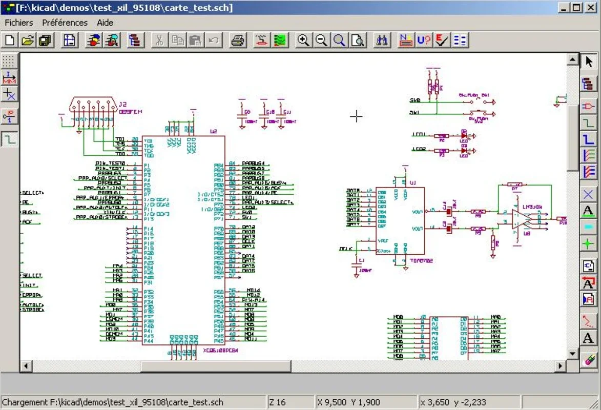
Eeschema (Schematic Editor): This intuitive schematic capture tool allows you to create both simple and complex hierarchical designs with ease. Its features include:
- Component Libraries: Access a vast library of pre-defined components, saving you valuable time and effort.
- Symbol Creation: Easily create custom symbols for unique components not found in the library.
- Hierarchical Design: Manage complex projects by breaking them down into manageable, hierarchical sheets.
- Netlist Generation: Automatically generate a netlist, a crucial step in transferring schematic information to the PCB layout stage.
- Electrical Rules Check (ERC): Identify potential design errors, such as shorts, open circuits, and incorrect component connections, before proceeding to PCB layout.
-
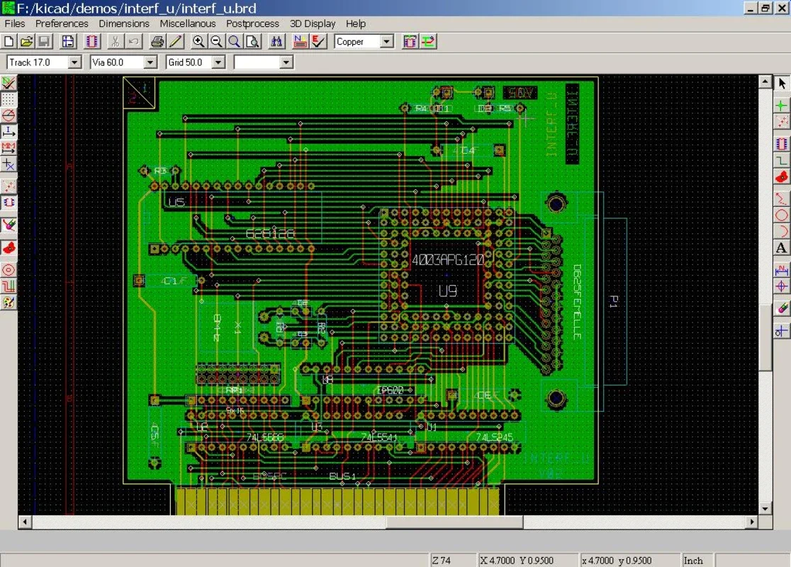
Pcbnew (PCB Editor): This robust PCB layout tool offers a wide range of features for creating professional-quality printed circuit boards:
- Automated Routing: Leverage Kicad's powerful automated routing capabilities to quickly and efficiently place and route traces.
- Manual Routing: Fine-tune the routing manually for optimal placement and signal integrity.
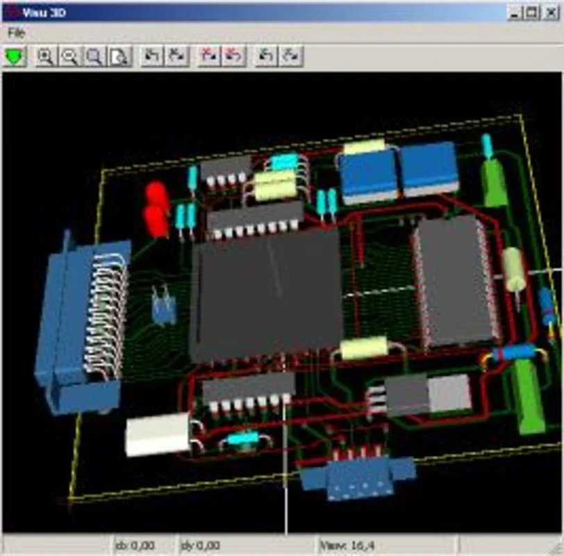
- 3D Visualization: Visualize your PCB design in 3D to check for clearance issues and overall design aesthetics.
- Design Rule Checking (DRC): Ensure your design meets manufacturing specifications by running DRC checks.
- Layer Management: Effectively manage multiple layers to create complex and sophisticated PCB designs.
-
Cvpcb (Component Association): This tool acts as a bridge between the schematic and PCB design stages. It automatically associates components from the schematic with their corresponding footprints on the PCB, minimizing the risk of errors and saving significant time.
-
Gerbview (Gerber Viewer): Once your PCB design is complete, Gerbview allows you to view and verify the Gerber files before sending them to a manufacturer. This ensures accuracy and avoids costly mistakes.
Workflow and Design Process
The typical workflow in Kicad involves the following steps:
- Schematic Capture (Eeschema): Begin by creating your schematic using Eeschema. Define components, connect them, and ensure the design functionality through the ERC tool.
- Netlist Generation: Once the schematic is complete, generate a netlist to transfer the design information to the PCB editor.
- PCB Layout (Pcbnew): Import the netlist into Pcbnew and begin placing components on the PCB. Use automated and manual routing to connect the components according to the schematic.
- Component Association (Cvpcb): Utilize Cvpcb to verify that components in the schematic are correctly associated with their footprints on the PCB.
- Design Rule Checking (DRC): Perform DRC checks to ensure the design meets manufacturing requirements.
- Gerber File Generation: Generate Gerber files for manufacturing.
- Gerber File Verification (Gerbview): Verify the Gerber files using Gerbview before sending them to the manufacturer.
Kicad vs. Other EDA Software
Kicad stands out from other EDA software packages due to its open-source nature, comprehensive feature set, and ease of use. While commercial packages like Altium Designer and Eagle offer similar functionality, they often come with high licensing costs, making them inaccessible to many users. Kicad provides a viable and cost-effective alternative without compromising on features or quality.
Compared to other open-source options, Kicad boasts a more mature and robust feature set, a larger and more active community, and extensive documentation. This makes it a preferred choice for both hobbyists and professionals alike.
Getting Started with Kicad
Kicad is available for Windows, macOS, and Linux. The installation process is straightforward and well-documented. The software is distributed as a self-extracting archive; simply download the archive, extract its contents, and run the executable file. No separate installer is required.
Advanced Techniques and Tips
- Keyboard Shortcuts: Mastering keyboard shortcuts can significantly speed up your workflow.
- Scripting: Kicad supports scripting, allowing for automation of repetitive tasks.
- Community Support: Leverage the extensive online community for support and assistance.
- Tutorials and Documentation: Kicad's documentation is comprehensive and easy to follow, providing ample resources for learning and troubleshooting.
Conclusion
Kicad is a powerful and versatile EDA suite that empowers users to design electronic schematics and PCBs with ease and efficiency. Its open-source nature, comprehensive feature set, and active community make it an ideal choice for both beginners and experienced designers. Whether you're a hobbyist working on a small project or a professional engineer designing complex systems, Kicad provides the tools you need to succeed. Its intuitive interface and robust functionality make it a valuable asset in the world of electronics design.